In this website, in documents and some communications via mail we usually adopt many technical terms because of they are a part of our business. In order to facilitate the communication we are used to employ abbreviations and acronyms which are international standard for PCB field; however, in order to be clearer for interested people, in this page there is a glossary with all technical terms and abbreviations employed with their meaning.


It’s the copper area on the pad that sorround the via when connecting to another layer, measured from the edge of the pad/via hole to the edge of the pad.
Example:
with the service FAST PCB the hole minimum size is greater than or equal to 0.35mm
The requiered minimum of annular ring is 0.20mm (pad size will be: 0.75mm=0.35+0.20+0.20mm)

It’s the traditional name of an electronic printed board which allow to assembly the components once built. A Printed Circuit Board, or PCB, is employed in order to mechanically support and connect electronical components using conductive lines, or traces printed on copper laminate with  non-conductive substrate.

This option will date the date code ww/yy to be added to the circuit board for increased traceability. Our standard process will add this in the silk screen, can be added in the copper layer if no silk exists or there is insufficient room.
Our Logo will be printed on solder mask bottom layer next to the data code always to improve the traceability.
The expression PB free will be added on the manufacturing lead free.
The number of conductive layers required for your pcb order.
Text such as company name, logo, or part number that is correct reading on the top copper layer will insure the layers are oriented correctly. This orientation text can be placed inside or outside of the board outline. Text placed outside of the board outline will be used for reference only and deleted prior to manufacture.
through our service Prod PCB it can be quoted up to 30-layers. If your board has a higher layer count, please complete our online Custom Quote personalized form.

The Industry standard format for files used to generate artwork necessary for circuit board imaging. PCB Online’s preferred Gerber format is RS274X, which places aperture information in the header of each gerber layer file. If files are not saved in RS274X, PCB Online will need one aperture list sent with the files. When your software outputs more than one aperture list we may place your order on hold until we receive your instructions or correctly formatted files.

This is an example of an Excellon drill file. It will have X & Y coordinates with tool sizes viewable in any text editor. This is the file that governs your finished hole sizes and locations.

A Sample Excellon File:

M48
;Layer_Color=9474304
;FILE_FORMAT=4:3
METRIC,LZ
;TYPE=PLATED
T01C0.300
T02C0.356
T04C0.635
T05C0.800
%
T01
X016685Y01045
X016765 Y000425
X004365 Y000425
X004285Y-03816
X0026Y02337
X016685 Y-03816
X016765 Y01045
T02
X00815Y000425
X02055Y01045
X0219Y001075

A patterned arrangement of printed circuitry and components that utilizes flexible base material (such as Kapton for example) with or without flexible cover lay.
Flexible circuit boards are often used as connectors in various applications where flexibility, space savings, or production constraints make the use of rigid circuit boards impossible. In addition to cameras, a common application of flexible circuits is in computer keyboard manufacturing; most keyboards made today use flex circuits for the switch matrix. Flexible circuits are available through the Custom Quote Service.

The process of adding solder to the exposed copper features of the circuit board. Finished boards are dipped in a molten solder bath and passed through a high pressure stream of hot air to remove excess solder, resulting in a uniform solder layer being applied to all exposed copper surfaces (all parts uncovered of solder mask).
RoHS is the acronym for Restriction of Hazardous Substances. RoHS, also known as Directive 2002/95/EC, originated in the European Union and restricts the use of specific hazardous materials found in electrical and electronic products. All applicable products in the EU market after July 1, 2006 must pass RoHS compliance.
In an effort to support the RoHS initiative, PCB Online offers several options that comply with the directive. All of the laminate material, soldermask material, and silkscreen material supplied are compatible for assembly at lead free solder temperatures and do not contain (above the upper limits) any of the restricted materials. There are several options for surface finishes for RoHS compliance: Immersion silver, ENIG (Full Feature only), OSP (Full Feature only), electrolytic gold (Full Feature only)
RoHS compliance applies only to the printed circuit board “as shipped” and PCB Online retains no responsibility for RoHS compliance of the printed circuit board after any subsequent processing or component placement by our customers or their assemblers.

In order to support the ROHS compliance, PCB Online have a variety of manufacturing in order to satisfy your requirements in building. Every our solutions of lead free PCB follow ROHS compliance and they have the same quality you are usual to expect from PCB Online.

In order to protect the pad from oxidation  and to improve the soldering we could build PCB with HAL Lead-Free on the contacts. The material employed is Tin (Sn).

ENIG (Electroless Nickel Immersion Gold)  is a chemical process, applied after soldermask drafting which add 3-6um of nickel before adding between 0.06um and 0.10um of gold over all copper surfaces uncovered by soldermask.

PCB will be delivered milled in single piece following the project supplied. The PCB will not delivered in a panel composed of more pieces for the automate assembly.

Printed circuit board delivered in a panel composed of more than one piece., following the Customer’s specifications file, or if there’s not, like our standard: 5.00mm breakway, 2.1mm holes on breakway and 1.5mm fiducial mark uncovered by solder 2.5mm size milled with witness microdrilled with the panel size such as a A4 format paper.

This method creates two beveled scoring lines along the perimeter of your boards. This makes it easier to break apart the boards at a later date. You would receive your boards in panel form like tab routing. Be sure to check with your assembly house for any special needs they might have. Be aware to specify at the moment of the order in the notes the will to obtain this kind of manufacturing (V-Cut), different from the standard PANEL PCB (witness with micro-drilling).

Defined as the size of the smallest drilled hole present in the design.

A PCB with copper printed on one layer only (usually copper would be on drill layer). Every hole will be not plated. The pad for soldering shall be oversized in order to provide an appropriate mechanical support for assembly (too much small pad, infact, could be easly teared up from pcb substrate).
With assembly technology SMD, copper layer is on the components layer, or on the top layer of the schede. In order to avoid that you project would be stopped, it needs to add a word text on copper layer (for example LS/LC or the code name of the PCB) to highlight it; this simple expedient will avoid the confusion about copper orientation allowing a correct drilling.

It’s the top layer of the PCB, the one in which the components are usually assemble, sometimes also called components layer (LC). However, very often on pcb the components are set up on both layers (top and bottom) so it’s more useful called it top layer.

It’s the opposite layer of the top one. The bottom layer of PCB is usually the one without components which pass over the wave soldering during the assembly. This is the reason why sometimes it’s called also solder layer (LS). However, very often the PCB have components on both layers and the assembly process do not require wave soldering. So it would be clearer called it BOT layer.

PCB with more than two copper layer are called MULTILAYER. In a multilayer PCB, the top and bottom layers are called outer layers. It’s useful to name them “outer layer” because of they are manufatured in different way and in the following phase they would be added to other copper layers.

Multilayer PCB are composed of a number of copper layers between the outer layers. These copper layers are called inner layers. The sequence to build the inner layer is very important and it’s determinated by their denomination. Usually it’s just a numeration from n. 2  and so on.
Below an example of 6 layers PCB denomination:
Strato •Top
INTERNO 2
INTERNO 3
INTERNO 4
INTERNO 5
Strato •Bottom

It’s important that the denomination and the exstension of file’s names which contain layout data are clear and complete for every PCB software and his engineers.

Surface mount devices (SMD) is a method of building the circuit board in which the components are assemble or set up directly on pcb’s surface without drilling. Anyway, PCB must be designed in a suitable mode in order to have the pad corresponded with SMD’s contact points.
an electronic device so built will be called Surface Mount Device (SMD). In the electronic field it has almost substitute the assembly with through-hole technology (THT).
Both kind of technology can be useful for the same PCB if it needs to assemble components not suitable to surface mount such as big transformers and semiconductor of power.
A SMT component is usually smaller than the opposite part with through-hole, it could have small plug or different kind of cables, flat contacts, ball grill array (BGA), or terminations on the component.

The thickness PCB is the thickness provided in mm of the base material sized without the copper laminate of the top and bottom layers. The PCB thickness doesn’t represent the final thickness of the printed circuit board, this is the reason why we would add a copper sheet and the finishing, solder mask, etc…

FR-4 (or FR4) is a grade designation assigned to glass-reinforced epoxy laminate which stands for flame retardant (self-extinguishing)

TG is the value (°C) which have to guarantee the mechanical stability of the PCB during its whole operative life. For our PCB, we usually use basic material with TG 145°-150°, upon request through special quote it’s possible to obtain a quotation for high TG material (such as Rogers 4350B with TG 280° C).

Many times PCB need to have particular areas protected during components’ soldering phase, in order to protect carbon or gold contacts. Peelable mask supply protection in many process such as wave soldering, reflow soldering, or hot air level soldering (HASL). Peelable mask (also called strippable mask or blue mask) works as protector during components assembly and it is removed after the process by the assembler himself. The designer can plan the peelable mask on every PCB, making a unique fluid piece which allow the Customer to detouch the whole protection with a single movement.

Carbon ink can be employed for keyboard’s contacts, LCD contact and small bridge. Print is done with carbon conductive ink.
It needs to follow some rules to obtain a correct result with this special material:
– Minimum carbon gap is 0.400mm (16mil)
– Minimum carbon line width is 0.300mm (12mil)

Ii’s a copper pad applied on PCB border, usually on the opposite angles or on breackway of the PCB and they are useful as reference for SMT process.

Last years, also thanks to components such as BGA (Ball Grid Array), FBGA (Fine BGA), UFBGA (Ultra Fine BGA) a new technology for printed circuits develop the so called blind holes and buried holes:


glossary_eng


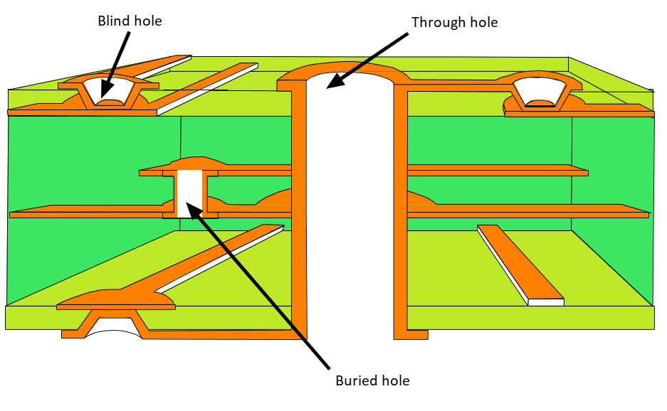
A blind hole is a standard vias hole PTH, but it links just a single outer layer with one or more inner layers, not passing completely through the PCB thickness, applied with a controlled depth on Z axis of the board. This procedure allows to obtain high density of connections for every surface unity and it becomes almost inevitable when the disigner needs to add on pcb components very innovative in small places. Blind holes with small size are made with laser of precision.

A buried hole is a PTH hole which links one or more inner layers, not connecting with outer layers, in this way the hole is completely buried in the PCB and invisible from the outside.
In order to realize blind holes and/or buried holes for your design it’s necessary to use the Custom Quote Service in which you can add file with specifications’ data about holes, specifying this special building procedure in Note (being a particular manufacturing, we have to judge the file in order to confirm the design feasibility and give you a custom quotation).

It’s useful to test shortcircuit and the opening of the printed circuits. All that can be tested is determined by soldermask., test points infact shall be exposed to solder, in general, endpoints of all of the nets are programmed for testing unless they are covered in soldermask. The standard testing parameters used are 100 Volts, Isolation Resistance of 10 M Ohms, Isolation Distance 0.050”, and Continuity Resistance of 50 Ohms. It’s not possible to accurately test boards that have silkscreen on pads. It is highly recommended that the silkscreen clip option be selected on electrically tested orders.
We recommend testing all surface mount boards and multilayer orders.
PCB Online, in order to guarantee the best reliability towards its customers, apply the 100% electrical test on every printed circuit board manifactured without additional cost.