PCB design guidelines

Introduction
These Guidelines set out best practice to reduce the cost of your boards and to minimize the risk of errors arising during manufacture process. Not all of the PCB design features are available on all our services. Look at our services overview to see more details.
Data format
Accepted format formats for PCB layout are:
|
Gerber RS – 274X (Extended Gerber with embedded apertures – developed by Gerber Systems) Gerber RS-274D (Standard Gerber with separate aperture file – developed by Gerber Systems) Layout PCB means all copper layers, soldermask, silkscreen, card profile or mechanical floor, pasta floors SMD, for carbon levels, peel-off plans, etc. Drilling: Excellon (1 or 2) + diameters list used (better if incorporated) Sieb & Meyer + Diameter list used (best if embedded) Gerber RS-274X or RS-274D format (plane with real-size holes, not a drill legend) DPF (plane with real holes, not a drill legend) IMPORTANT: Please provide only ASCII-coded files. This type of file is readable by our engineers and can be verified visually, if necessary, during data preparation. Design data The Gerber size is clear and unambiguous. It has been the industry standard format for PCB production for many years. Every PCB design software can produce Gerber data (the process will be fully described in the manual CAD PCB or in the help file). You can also check the accuracy of generated Gerber output data by downloading one of the many free Gerber viewers available on the internet.
|
Data requirements to be sent
The preferred data formats are:
For all PCBs layer — Extended Gerber (RS-274X)
For drilling — Excellon1 + Diameter list used (built-in)
F ornire only the data files nec essari for production. These are:
Gerber files for copper layers, soldermask and legend layers, mechanical layers and SMD paste layers. In addition to carbon, peel off and via-fill layer if necessary.
Excellon drill file to drill.
Please do not provide any additional files such as original CAD data, Graphicode GWK files, Excel (.xls) file, Part Lists, positioning and assembly information, etc.
Where you can contr ollare the output data generated (Gerber & Excellon files) using a Gerber viewer before sending it to production. Make sure that all the instructions for understanding the PCBs are included in the Gerber and Excellon files.
Try using a simple file naming and try to avoid long file names. Make sure that you can easily determine the function of each layer from the filename.
The files that are required to complete a certain order, depend on the number of circuit layers and the possible options. In this section you can find the complete list of the files needed for the various products marketed by PCB-PROTO. The files are of three types: required, dependent on the number of layers and optional.
Recommended name:
- . gko – gerber files mechanical floor
- . drl – ASCII Drill file (Excellon o Sieb & Meyer)
- . GTL – gerber side TOP
- . gbl – gerber side BOTTOM
- .gl1 – first layer gerber (immediately under the top)
- .gl2 – gerber per second inner layer (just above the bottom)
- .gl3 – gerber for the third inner layer (just above the fourth inner layer)
- .gl4 – gerber for the fourth inner layer (just above the bottom)
- . gts – gerber for the TOP of the solder mask (if required)
- . gbs – gerber for the BOTTOM of the solder mask (if required)
- . gto – gerber for the TOP screen printing (if required)
- . gbo – gerber for the BOTTOM of the screen printing (if required)
- . Apr – Openings of the imagesetter (only RS274D)
- . tol – the tips of description files (if not present in the drill file)
Holes
All sent files containing the drill bit diameters are always read by our CAM systems as the size of the finished hole.
All PCB production tips are manufactured in 0.05 mm increments. So we convert the size of the holes in millimeters to the nearest 0.05 mm.
For example:
The 31mil tip is converted to 0.7874mm and then rounded to 0.80mm.
The 32mil tip size is converted to 0.8128mm and then rounded to 0.80mm.
The 33mil tip size is converted to 0.8382mm and then rounded to 0.85mm.
If possible, provide drilling files with separate metallic (PTH) and non-metallic (NPTH) holes. If this is not possible, specify clearly which holes are PTH and which holes are NPTH.
When we do not receive any information about the type of PTH / NPTH holes we use the following rules to determine PTH / NPTH:
For single-chip circuits: All holes are considered as NPTH by default.
For double face and multilayer circuits: All holes are considered PTH except the following cases which are considered NPTH:
Holes unconnected and without plots of copper.
Holes not connected where the size of the copper pad is equal to or less than the hole size (the pad will be removed in preparation of the data)
Hole connection with a copper pad on 1 side (external), no connection on any other level (external or internal) and no copper pad on the opposite (outer) side.
The VIA holes <= 0.45 mm (18mil) are considered metallized as the default. The VIA holes have a maximum largest negative tolerance of the holes of the compo nents of this to optimize l ‘annullar ring when necessary. If you need component holes of 0.45 mm or smaller with standard component bore tolerances, you can specify this in order details.
IMPORTANT:
In order to allow metallization in the hole, it is necessary to drill before the metallization with a larger size punch (drilling oversize) of the required finishing hole, the ENDSIZE finishing augmentation rules for TOOLSIZE production are:
+ 0.15 mm for metallic holes (PTH)
+ 0.05 mm for non-metallic holes (NPTH)
S tandard tolerances on the diameter of the hole finished ENDSIZE.
NPTH holes + / -0.05 mm (+ / -2mil)
PTH holes + / -0.10 mm (+ / -4mil)
VIA holes have a maximum negative tolerance of 0.30 mm (12mil).
When no tolerances are specified in the data, we produce according to our standard tolerance specifications.
If you need tighter tolerances, you must clearly indicate the list of diameters and mechanical plane. (Increase the cost of the PCB so it should not be used without a valid reason).
The holes which overlap with the contour of the edge card may be:
NPTH holes without copper pad: These NPTH holes will be considered as part of the card profile.
PTH holes with copper pad: these will be considered as “metallic partial holes on the edge” and should be clearly indicated in the mechanical plane.
Observation: “metallic partial hole on the edge” are not available for the BEST PCB service.
Overlapping drill holes
Never overlap holes, these can cause the puncture to break in production and the small pieces of material left by the breakage can cause voids or shrinkage in the borehole. The minimum distance between the holes is 0.25mm (10mil) this is measured by hole hole edge on the TOOLSIZE drilling diameters.
Copper Spacing

| BEST-PCB | The minimum distance between the tracks and / or pitches must be greater than or equal to 0.18mm (7 mils). |
| FAST-PCB | The minimum distance between the tracks and / or pitches must be greater than or equal to 0.15mm (6 mils). |
| PROD-PCB | The minimum distance between the tracks and / or pitches must be greater than or equal to 0.15mm (6 mils). For this service it is possible to have a minimum insulation of up to 50 μ (with quotation on request) |
Track width
| BEST-PCB | The track minimum must be greater than or equal to 0.18mm (7 mils). |
| FAST-PCB | The track minimum must be greater than or equal to 0.15mm (6 mils). |
| PROD-PCB | The minimum distance between the tracks and / or pitches must be greater than or equal to 0.15mm (6 mils). For this service you can have a minimum track up to 50 μ (quoted on request) |
Annular Ring and Minimum drill size
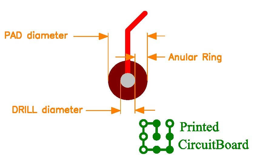
| BEST-PCB | The minimum size of a hole must be greater than or equal to 0.40mm. Annular ring minimum 0.25 mm |
| FAST-PCB | The minimum size of a hole must be greater than or equal to 0.35 mm. Annular ring minimal 0.20mm |
| PROD-PCB |
The minimum size of a hole de ve be greater than or equal to 0:30 mm. For this service you can have a minimum annular ring of up to 50 μ (with prices on request) |
- Since the ring ring has a great influence on the weldability, we recommend using a minimum (0.25 mm) ring ring at vias only.
- For example, a vias with a diameter of 16 mils (0.4 mm) must have a corresponding PAD with a diameter of ALMENO 28 mils (16 + 6 + 6 mils = 28 mils = 0.71 mm)
- IMPORTANT: The ring ring is calculated on the diameters of the drill bits (TOOLSIZE) and not on the diameter of the finished holes (ENDSIZE).
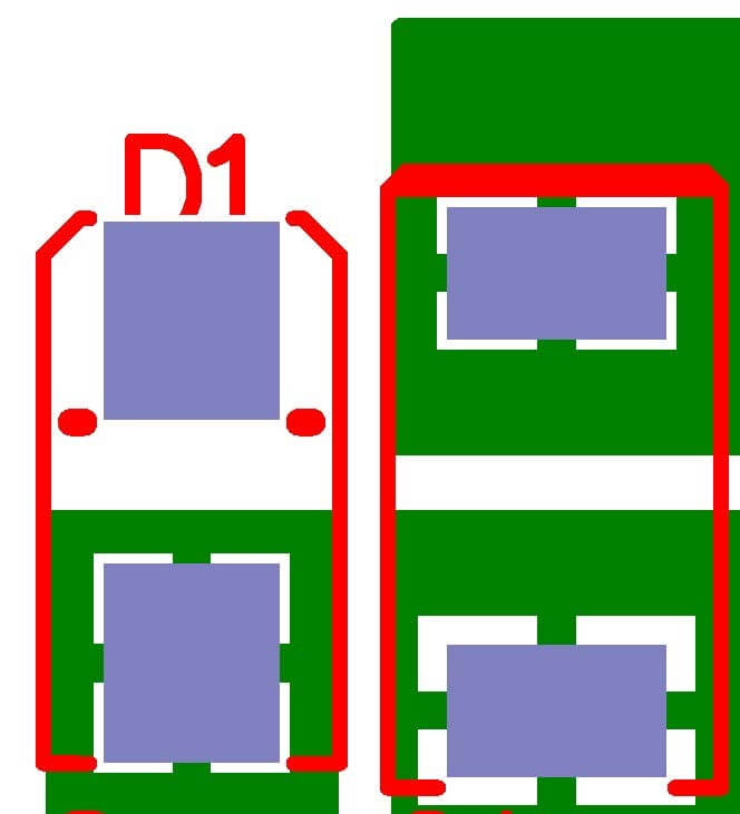
Annular rings on oblong pads
The rules for annular ring on oblong pads are no different from those of round plots, but allow some exceptions to the rule.
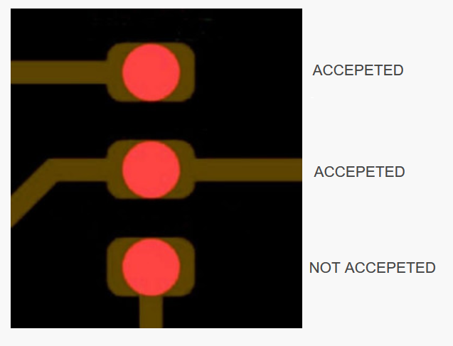
PTH hollow oblong pad:
The measures below are taken from the TOOLSIZE production.
- On the shorter side of the oblong pad the hole diameter must be> = 0:00 mm (0mil) (ie no breakout is allowed)
- On the longer side of the oblong pad in both directions the rim must be> = 0.300 mm (12mil)
ACCEPTED ANNULAR>=0.00 MM

NOT ACCEPETED ANNULAR<0.00mm

The hole can not be positioned in such a way that it could disconnect the track pad:
SOLDER MASK
When generating output data for soldermask,there is no need to oversize or compensate the soldermask pads. It is better to leave the soldermask pads at the same size as the copper pads.We will then set the soldermask to suit the technological needs for proper production and assembly of the boards.
The standard for all services is 0.100 mm (4mil) on the beam.
For the PROD-PCB service it is possible to have, on reporting, a smaller standard.
Pad solder = Pad Copper

Pad solder update to 0.1 mm on the radius

Silkscreen Printing
The minimum width of the line you use to draw the component overlay on the PCB must be : 0.17 mm (7mil)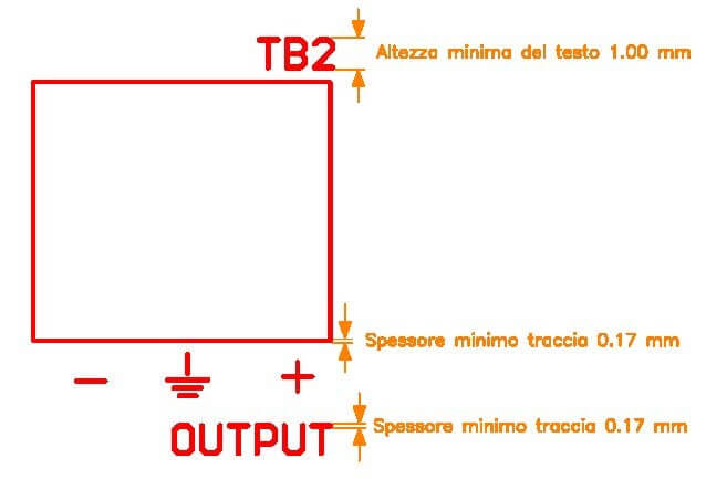
Minimum Text height for good readability 1.00 mm (39.5mil). The Legend Print will always be broken – or clipped – against the corresponding soldermask layer. Legend clipping clearance is 0.10mm (4mil). This means that we clip the legend 0.10mm (4mil) back from the soldermask openings , any bits of line smaller than 0.17mm (7mil) are removed or brought to the minimum.
In absence of a soldermask layer, the legend print is clipped against the corresponding copper layer. If there is no copper layer, the legend is clipped against the drill layer.
DESIGN TIPS:
To avoid your legend being clipped maintain a minimum distance of 0.20mm (8mil) between your legend elements and the copper image. This 0.20mm (8mil) = 0.10mm (4mil) Soldermask Annular Ring + 0.10mm (4mil) Legend Clipping Clearance.
All legend text must be correctly readable. As a PCB is always viewed from top to bottom through the PCB, text on the top layer of your board should be readable and text on the bottom layer should be non-readable or mirrored.
It is not advisable to place a legend layer on the copper layer side of a PCB without a soldermask layer.
MECHANICAL LAYER
Always include a Gerber mechanical layer in your data set.
A proper mechanical layer is VITAL to a good and flawless production of the PCB as it should provide us with all the needed mechanical information for the construction of your PCB. In case of cut-outs or slots in your PCB, this layer is essential to the production! DO NOT scale your mechanical layer, it should be 1 to 1 and reflect the exact dimensions of the PCB. The mechanical layer is – as for all layers – also viewed from top to bottom through your PCB, so do not mirror the mechanical layer. ONLY include information in your mechanical layer that is needed. Do not provide actual routing layers for board contours or inside milling.
Routing data is production-specific depending on the rout tools, tool compensations, routing order and direction used by each PCB fabricator. This means that we cannot use customer-provided routing layers. We need to completely rework them, which can lead to confusion and misinterpretations which may result in incorrect boards. It is our job as board producers to prepare correct production routing layers based on the information in your mechanical layer.
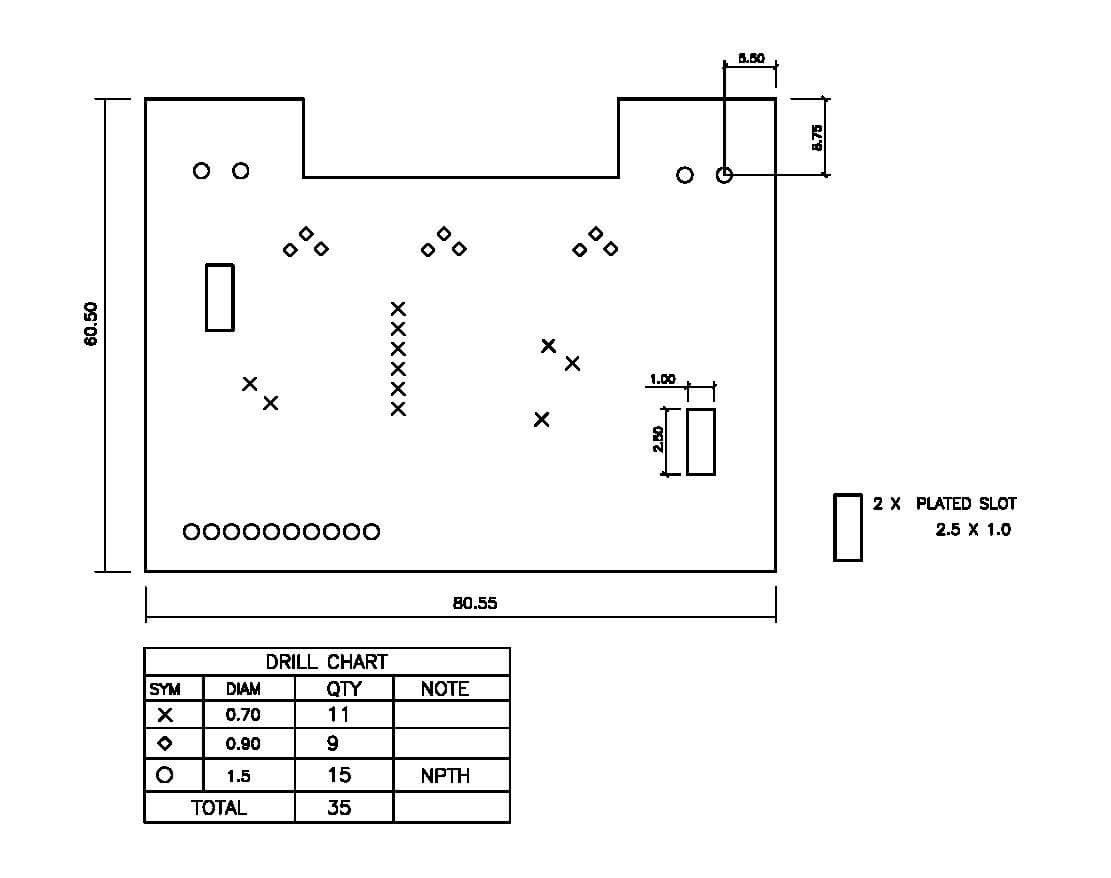
A mechanical layer should minimally contain:
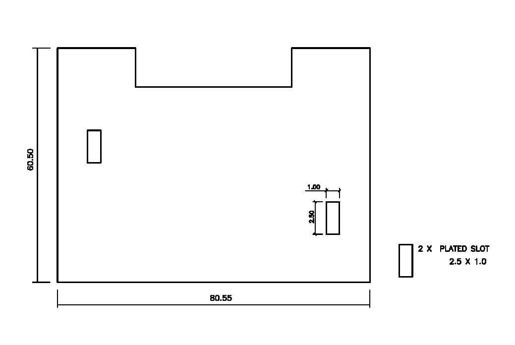
The exact board outlines, ideally including dimensions (mm or inch). Exact positions and sizes for all inside milling, slots or cutouts, ideally including dimensions (mm or inch).
IMPORTANT:
When no dimensions are given we will always take the center of the contour lines to be the exact outline of the board, regardless of their thickness. Additional information that should be included in the mechanical plan when needed:
A reference hole: the distance from one drill hole in X and Y to the PCB outline. This is particularly important when you only have NPTH holes without copper pads. Positional indication of all drills using symbols (=drill map). Use different symbols for each different drill size. PTH/NPTH indication for holes and slots ,If you supply panelized data include proper indications for break-routing and/or scoring (V-cut). A clear layer sequence or buildup drawing including all copper layers, soldermask and legend layers, any additional layers like peel-off or carbon, in the correct sequence viewed from top to bottom and with the correct corresponding data file name.
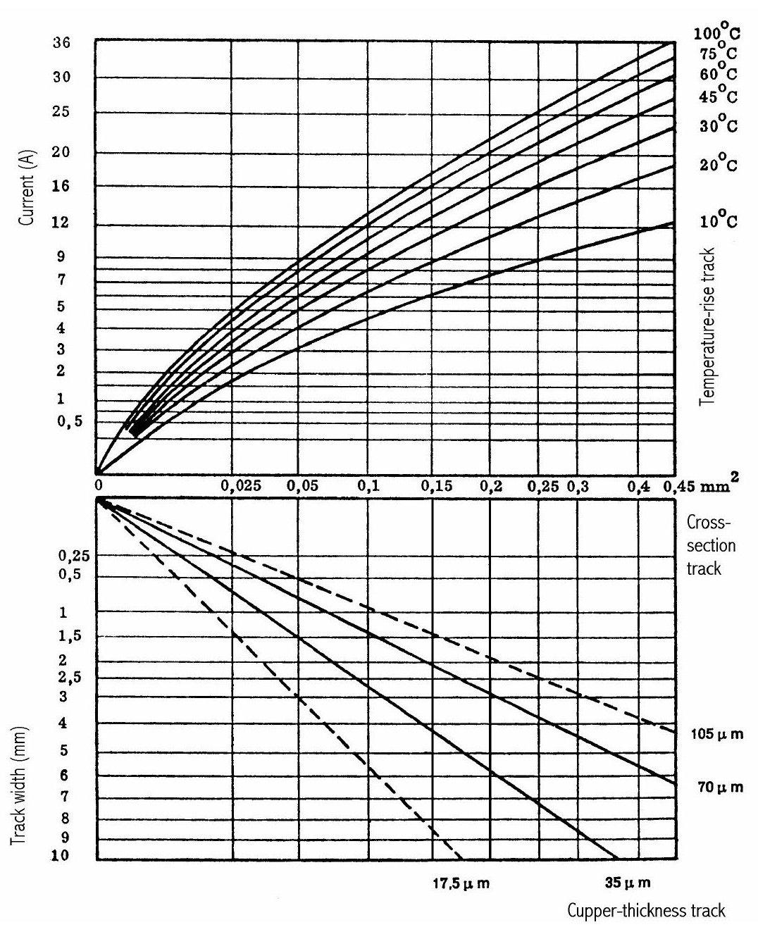
TRACK WIDTH GRAPHIC
The table below represents the extent of the slopes according to their section.
Additionally, depending on the allowed temperature increase (for Joule effect), you can increase or decrease the conductor section.
For example, the signal paths (project 1 and 2) have a width of 12mils, the thickness is 35μm. The current flow that allows a maximum temperature variation of 10 ° C is about 0.8A. This value is overwhelmingly overwhelming. In theory, the width of the tracks could be reduced up to 1mils (125mA range). In fact, this is not so often realized as processes for creating 1 mils are more expensive.
The feeding slopes have a width (normally) of 30 to 60 mils or even more (depending on the project).
Considering a thickness of 35 μm and a maximum temperature increase of 20 ° C, the flow rate of these will go from 2.5 to 4A.
For the sizing of particular cases refer to the table below